Hello! I'm TR of R&D department.
In this article, I’d like to explain about our development of NiFe alloy plating / electroforming technology which is applied to the formation of thin films and microstructures required to be metallic materials with the low coefficient of thermal expansion(CTE), such as molds and structures used in processes with large temperature changes.
Nickel-iron alloy plating that solves the problem of CTE mismatch
The various materials used in electronic devices have different coefficients of thermal expansion. Differences in the CTE between materials deteriorate the product yield in the manufacturing process, and cause defects or shorten the life depending on the environment in which the product is used.
Generally, the CTE of inorganic substrate materials such as silicon, glass, and ceramics is small. On the other hand, compared to that, the metal material used for wiring formed by plating or etching has a large CTE, and the resin materials such as epoxy and polyimide used for insulation show even larger values, so it is essential to consider the coefficient of thermal expansion when selecting materials on the design of electronic device products.
Coefficient of thermal expansion (CTE) control for NiFe Invar plating
NiFe alloy is a special material whose thermal expansion characteristics and magnetic characteristics change depending on its composition.
NiFe alloy plating / electroforming is applied to the formation of thin films and microstructures that are metallic materials and want to keep the coefficient of thermal expansion low, such as molds and structures used in processes with large temperature changes.
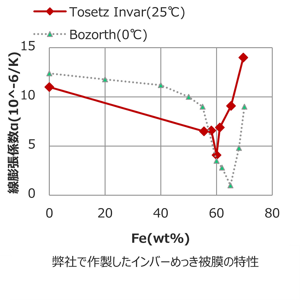
The coefficient of thermal expansion (CTE) of NiFe alloy shows peculiar behavior depending on the composition.
The 36% Ni-Fe alloy is called “Invar” and has a CTE of about 2ppm / K, which is as low as silicon. We have achieved a value of 4ppm / K, which is close to the literature value for Invar alloys, by the plating method.
We are also developing equipment technology that enables film formation with high film thickness uniformity and composition uniformity from silicon wafer size to substrate sizes exceeding 500 mm square.

Application fields of low thermal expansion plating
There are three points to consider when considering nickel electroforming.
1.MEMS
Electrode formation by plating and electroforming technology are also applied to MEMS. By controlling the composition ratio of nickel-iron alloy according to the application and purpose of the device, it is possible to form a plating film or structure with low thermal expansion characteristics and high magnetic permeability characteristics.
2.Power device
Next-generation power devices such as SiC, GaN, and gallium oxide are required to operate at high temperatures and high current densities, and various bonding technologies have been developed. The application of laminated metal film Copper-Invar-Copper (CIC) cladding for the purpose of matching the coefficient of thermal expansion is being studied.
Similarly, plating method that allows the lamination of dissimilar metals at room temperature can be applied. In the plating process, the coefficient of thermal expansion can be accurately controlled by changing the nickel and iron plating solution composition and current conditions. In addition, it is possible to form a laminated structure with copper plating in multiple layers with any film thickness. We expect for the possibility of a low thermal expansion electrode forming process by electroplating suitable for power devices.
3.Fine Metal Mask (FMM)
In the manufacturing process of organic EL displays(OLED), metal masks are used to deposit organic EL light emitting materials on glass or film. Nickel electroforming has been used in the manufacture of metal masks, but there is a limit to miniaturization because the dimensions change due to temperature changes. By applying Invar plating to electroforming, dimensional changes due to heating can be minimized, leading to improved quality and productivity of large, high-resolution organic EL displays.

Lastly
What do you think?
At Tosetz, we support the development of new products for our customers with technology that enables film formation with high film thickness uniformity and composition uniformity from silicon wafer size to substrate sizes exceeding 500 mm square!
Click here if you are interested in Tosetz.
↓

Comments