Hello! I'm TZ of sales department.
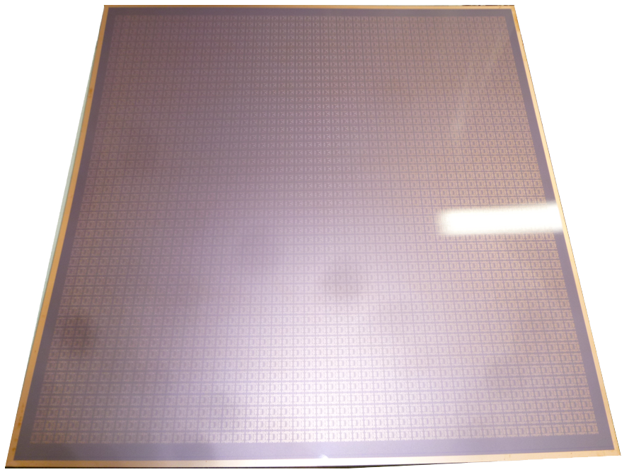
We received an order for an automatic transfer type double-sided electroplating tool for a 380 mm square substrate for a mass production line of a certain electronic device manufacturer in Japan.
High film thickness uniformity within ± 10% is required in the plating wiring and electrode forming processes of electronic components, but it is difficult to achieve it with conventional plating equipment for large substrates. But we have the know-how to realize high film thickness uniformity (± 2%) cultivated in face-up plating equipment for magnetic thin film process and we also provide our customers with plating equipment for large substrates. I am very grateful for the adoption of our tool product.
So let me explain why our plating equipment was selected by the customer.
Challenges for increasing the size of wafers to rectangle substrates
In order to develop highly market-competitive electronic device products, it is necessary to achieve both high performance and low cost. For inexpensive products in the volume zone such as smartphones and in-vehicle devices, a production line will be constructed with a larger work size for the purpose of reducing production costs. At the same time, ensuring a high yield is an issue.
In semiconductor packaging and small electronic component modules, increasing the size of the substrate from the wafer to the square substrate is being considered. But misalignment due to thermal expansion of the material used, warpage of the substrate and in-plane uniformity are the critical issues in fine wiring process. Currently, many material manufacturers and equipment manufacturers are engaged in research and development, and the supply chain building is proceeding.
In the process of plating wiring and electrodes for electronic components, high film thickness uniformity within ± 10% is required. At the same time, high-speed plating is required to increase productivity. There is a trade-off relationship that the thickness uniformity deteriorates so it’s important to optimize the process conditions and equipment conditions.

Many delivery records of vertical dip type equipment and timely demo evaluation
We have a track record of being adopted in many mass production factories of vertical dip type equipment for wafers of RF electronic parts in the past, but before introducing the equipment, we made experimental machines with the same specifications as mass production equipment and evaluated them for demonstration. We will propose the design of the most suitable mass production equipment for wiring / electrode formation by electrolytic plating based on the experimental results from the aspect of the process, such as the flow of plating solution, stirring method, structure inside the tank, resist pattern dependence, matching with plating solution composition, etc., to meet the required specifications.
We will do a demo evaluation of the square substrate!
We have prepared an environment where you can perform demo evaluation of square substrate. When considering the investment of plating equipment, we can also assist you in setting process conditions. After conducting a demo evaluation to verify the feasibility of the customer's required process and confirming the actual equipment performance, we will propose the optimum specifications according to the budget.
Process method to replace printed circuit board: FO-PLP
In recent years, fan-out panel level packages (FO-PLP) have been actively developed as an alternative to conventional printed circuit boards. The substrate size used for production is expected to be approximately 500 to 700 mm square for applications such as Cu pillar and rewiring layer (RDL) formation by copper plating and electrode (bump) formation by nickel / gold plating.
We are also studying large-scale substrate plating equipment for electroplating of nickel and Invar alloys that show a low coefficient of thermal expansion (CTE), aiming at new growth market fields. It is expected to be applied to fine metal masks of MEMS and organic light Emitting Diode (OLED).
Lastly
What do you think?
Tosetz can also handle double-sided plating of large square substrates!
If you have any problems, please feel free to contact us.
↓

コメント